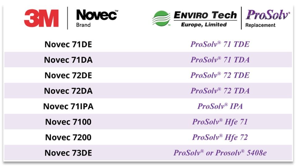
NOVEC REPLACEMENTS SOLUTION

W H Y are semiconductors so important to so many industries?

How Is a Semiconductor Manufactured?

Silicon wafers

Silicon wafers provide the foundation for semiconductor devices. The process begins when a pure silicon crystal (an “ingot”) is sliced into thin wafers and polished to smoothness. Polishing the wafer eliminates impurities and scratches, leaving a good base for fabricating chips. This step is critical, for even slight contamination can cause product defects. After the polishing step, a blanket of conducting or semiconducting materials is deposited onto the wafer—a step referred to as “deposition.”

Download now

After preparing the wafer, its surface is coated with a photoresist, a light-sensitive material that changes the chemical properties of the wafer to make it suitable for circuit printing. There are two main types of photoresists (or resists) based on their ultraviolet light (UV) reactivity: positive and negative.


When exposed to UV light, positive photoresist becomes soluble, dissolving exposed resist and leaving unexposed resist remaining. Conversely, negative photoresists harden when exposed to UV light. Due to superior thermal stability and resolution capability, positive photoresists are more commonly used in the semiconductor manufacturing process.

Talk to an expert

Advanced Optics

After coating the wafer with photoresist film, it’s ready for circuit printing. The process of drawing a circuit design onto a wafer is called photolithography. In this step, the wafer is inserted into photolithography equipment, exposing it to UV light. In the lithography machine, light passes through a mask containing the blueprint of the circuit, printing the pattern on the wafer coated with a photoresist film. Refraction and defects can occur in the lithography process, which is why robust quality control is necessary.

Learn more

After printing the circuit diagram on the wafer, etching follows to remove any excess materials from the surface. This process can be done in two different ways:


  1. Wet Etching with chemical solutions in the etching process
  2. Dry Etching using gases or plasma

Because semiconductor chips have many layers, the photolithography and etching processes are repeated several times on every layer of the wafer to create the final product. The entire procedure requires precision and close process control to avoid damaging the chip structure.

Contact us

Impurities (such as arsenic or phosphorous ions) are embedded through ion implantation to give silicon wafers semiconducting properties. Then, heat processing is conducted to activate the ions and create micro-transistors. The photoresist material blocks the ions from entering areas that could lead to defects and is removed after implantation by ashing or using chemicals.

Item Link

The entire semiconductor manufacturing process can take up to 26 weeks, from design to production. The last stage of the production process entails separating the wafer into individual chips (dicing) and placing the chips onto a substrate through bonding. Finally, a protective metal container with a cooling system is placed on top of the chip to ensure it doesn’t overheat. After this process, the chip is ready for use.


The semiconductor manufacturing process entails several other steps, including testing and inspecting the chips. Some of the most common challenges manufacturers face are the following:


Product Quality: Ensuring product quality can be challenging as semiconductor products become more advanced and demand grows.


Defects: Several steps, from assembling to testing, can lead to product defects. These defects can be hard to spot, considering each chip’s size and number of layers.


Cost: The cost of the semiconductor manufacturing process is rising as new technologies emerge and shortages occur, making it harder for manufacturers to break even in revenue.


Equipment: Advances in the industry will require manufacturers to keep up with new equipment and technologies, which can be a struggle and an added cost.


Time: Even minor problems in the production process can ruin an entire batch of chips, and it can be a struggle to minimize downtime when quality is compromised, and delays occur.

Item Link

What Is Semiconductor Manufacturing?

Transforming silicon and/or other raw materials into semiconductor devices is a complex process that can take months to complete. Semiconductor manufacturing is the fabrication method used to create integrated circuits (IC), consisting of transistors and other components that are built into modern electronic devices. The process is made up of multiple chemical and photographic processing steps that transform a wafer of semiconducting material into electronic circuits. What raw materials are needed for semiconductors? Typically, manufacturers use pure elements like silicon or germanium as semiconducting materials.

Learn more

What Is Required for Semiconductor Manufacturing?

The fabrication process includes three main areas: wafer creation, circuit construction, and packaging. Below are the most essential components required in the process.

Raw Materials like silicon or compounds

Gases like nitrogen, oxygen, and argon to create the proper environment and chemical reactions to shape the semiconductor’s electrical properties

Semiconductor Manufacturing Equipment, including dicing machines, probing machines, edge shaping products, and grinders

Quality Control Equipment like optical inspection systems, to ensure product quality

Learn more

Semiconductor Grinding, Lapping, & Polishing Systems

Stock Removal and Nano Grinding 

By adopting a stock removal and or nano grinding approach, surface roughness figures of 2nm Ra can be achieved therefore facilitating the capability to go straight to CMP after grinding.


Learn more about it

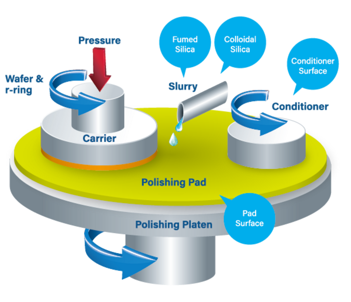
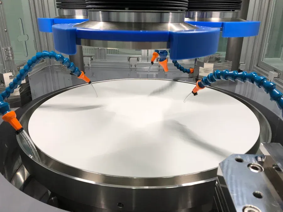
CMP Chemical Mechanical Polishing 

Post-Grinding Engis offers specifically developed machines and consumable products capable of efficiently producing Epi surfaces on virtually all semiconductor materials. 

Semiconductor Wafer Grinding & Back Thinning


  • SiC
  • Si
  • AI203
  • GaN
  • GaAs
  • InP
  • AIN
  • Others


Book a consultation